The technology narrative of DRAM is beginning to diverge. After ChangXin Memory Technologies disclosed progress on its next-generation 4F² architecture and products, Samsung confirmed it will continue parallel development, SK Hynix chose a gradual approach, while Micron explicitly stated it will not follow.
ChangXin explicitly regards the 4F² architecture as one of the opportunities for "overtaking on the curve." Its judgment is that ChangXin and the three major overseas DRAM manufacturers are all in the exploration stage with this new technology, and commercialization still carries uncertainty.
ChangXin Memory Technologies aims to overtake on the curve via IPO
2026/05/18 Read in full>
One of the core goals of DRAM process competition is to increase the storage bit capacity per unit area. The theoretical planar footprint of a single DRAM memory cell can be simplified as kF². Under this formula, increasing storage density comes down to two paths: reducing the layout coefficient k, or shrinking the feature size F.
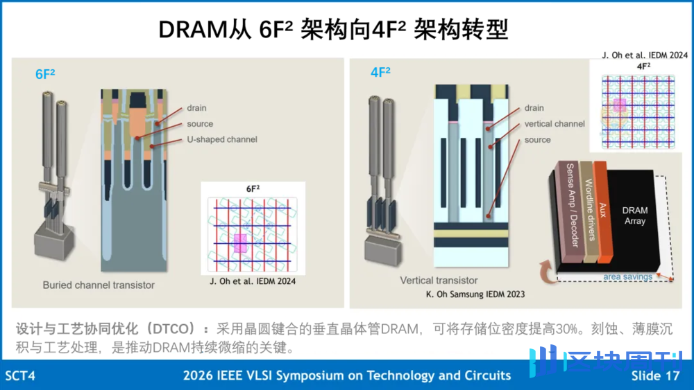
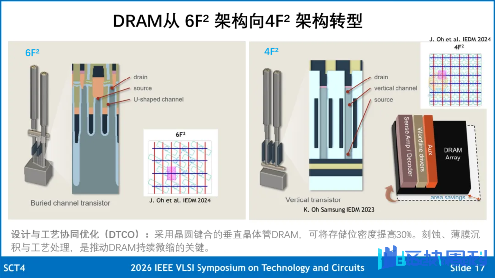
Note: From 6F² to 4F², the theoretical planar footprint of the memory cell (the pink area in the figure) shrinks from the typical 3F×2F to 2F×2F
About twenty years ago, the industry once compressed the cell area from 8F² to 6F² by changing the memory cell layout. For a long period thereafter, DRAM density improvement mainly relied on continuous shrinking of the feature size. Today, as planar scaling becomes increasingly difficult, architectural innovation to reduce k has once again become an important direction of industry competition.
But clearly, this time, the industry has not yet formed a clear technical consensus. Different manufacturers are making different judgments on the technical feasibility, economics, and commercialization timing of 4F². This also provides ChangXin with a competitive window different from the past.
From ChangXin's first publication of papers related to the 4F² architecture in 2021 to further discussion of its technical challenges at IMW 2026 (IEEE International Memory Workshop) earlier this year, the market has long known that ChangXin has placed a heavy bet on the 4F² route.
Even so, few expected its progress to be so rapid. On October 10, ChangXin announced that it expects to launch a new-generation DDR5 RDIMM product integrating the 4F² architecture and hybrid bonding technology by the end of the year, and will advance the pace of mass production according to customer validation progress and market demand. This caused sharp declines in the stock prices of South Korea's Samsung Electronics, SK Hynix, and the United States' Micron; of course, the overall cooling of the AI narrative was also a factor.
On the 14th, at an industry exhibition, Song Jaehyeok, Chief Technology Officer of Samsung Electronics' Device Solutions (DS) Division, confirmed that Samsung is working to advance the 4F² architecture. Earlier this year, the company showcased a 16Gb 4F² DRAM test chip using the corresponding technology. It is said to enter mass production in 2028.
On the 21st, Scott DeBoer, President and Chief Technology and Product Officer of Micron Technology, publicly stated that the company will continue to extend the 6F² architecture while advancing 3D DRAM research and development, and will not include 4F² in its current technology roadmap. Micron was once a pioneer of the 6F² architecture and has already studied 4F² for more than 20 years, yet now believes that this direction is both expensive and difficult, lacking a sufficiently attractive path to scale.
On the 28th, during an earnings call, SK Hynix confirmed that it will transition to the 4F² architecture, but this is not the company's focus at the current stage. The current R&D plan is to fully leverage the potential of the 6F² architecture as much as possible through process maturity and a stable technology platform, and to extend the lifespan of that technology platform. SK Hynix hopes that each technology will be applied to the right product at the right time. The "right time" here includes both technical readiness and economic readiness.
All of this is just as ChangXin judged in its prospectus: 4F² is still in the technology exploration stage, and there is still uncertainty before large-scale commercial application. Each company's scaling capability, process environment, and cost structure differ, so their strategic choices regarding the 4F² architecture also differ.
Micron's concerns are not without reason. Theoretically, at the same feature size F, 4F² can reduce the planar footprint of a single memory cell by one third, increasing the number of memory cells that can fit in the same area by 50%. But going from 6F² to 4F² is not simply compressing the cell area; it is a re-layout of the DRAM cell's 1T1C structure. It not only needs to ensure memory performance but must also meet yield, reliability, and cost requirements.
During more than 20 years of two-dimensional scaling, the capacitor (C, capacitor) has been stretched into a tall, thin cylindrical shape so that it can still store enough charge in an ever-shrinking space. To reduce the typical 3F×2F architecture of 6F² to the 2F×2F of 4F², the transistor (T, transistor) also needs to be stood upright, which means new device structures and integration processes.
However, Micron believes that the transistor layout can be changed, but capacitors cannot be brought infinitely close, because sufficient capacitance, insulation performance, and manufacturing reliability must be ensured.
This means that the theoretical density gain of 4F² will be significantly discounted after accounting for capacitor spacing constraints, peripheral circuit area, and redundant cells, while process costs are rising. So whether its economics are better than continued scaling of 6F² is not self-evident. Moreover, even if everything goes smoothly, it is still constrained by yield improvement and capacity ramp-up speed, which will erode profits for a long period.
The market is so hungry for DRAM that even Altman raised a controversial question: why let large amounts of memory sit idle in personal computers. Micron believes the shortage will last until 2028, and SK Hynix even expects it to last until 2030. In such a market environment, for giants that already hold larger market shares, investing large amounts of capital and R&D resources into 4F², whose commercialization prospects are still unclear, is not the most attractive choice at present.
They have EUV (extreme ultraviolet lithography) and can improve density through continued shrinking of F, fully squeezing the value of the 6F² process during this period of high DRAM premiums; Micron is the latest among the three to introduce EUV into DRAM mass production, and the processes it accumulated earlier in the DUV multiple patterning era also provided a foundation for its subsequent adoption of EUV.
ChangXin's limitation lies in its lack of advanced lithography capabilities such as EUV. If it continues along the 6F² route, it will need to continuously shrink the feature size F and rely increasingly on DUV multiple patterning, and its economics will inevitably be squeezed by overlay accuracy, process windows, and yield.
4F² may change this constraint relationship, giving ChangXin the opportunity to use a relatively larger feature size F, thereby reducing dependence on extreme lithography and multiple patterning. If this structural advantage can be realized in actual processes, mass-producing DRAM with the 4F² architecture may be more cost-effective than continuing to rely on DUV multiple patterning to scale 6F².
This is equivalent to gaining a time window for the development of domestic advanced lithography equipment. This is also why Chinese semiconductor manufacturers, while also researching next-generation chip technologies such as 3D folding and 4F², may push such technologies from the laboratory to productization earlier and more actively than industry leaders. Because they have no choice, and they do not carry too heavy a historical burden. This is innovation forced into existence, and of course, it is also fraught with difficulties.
But the "overtaking on the curve" from 6F² to 4F² is essentially only a one-time structural dividend. After compressing the cell area to 4F² by changing the layout coefficient k, further increasing DRAM capacity density still requires shrinking the feature size F.

In fact, 4F² is not the long-term technical endpoint of the DRAM industry, and may not even necessarily evolve further to 2F²; rather, it is a阶段性 choice in the exploration of next-generation memory architectures. The DRAM technology roadmap proposed by Applied Materials includes, in addition to 4F², advanced lithography-driven scaling, advanced peripheral transistors and interconnects, CMOS bonded arrays, and 3D DRAM. These directions are not mutually exclusive.
In the long run, the path to 3D DRAM is an important direction for the industry to break through the density limits of planar arrays. Unlike 4F², which adjusts the layout within a 1T1C memory cell, 3D DRAM stacks multiple 1T1C memory arrays vertically.
Advancing 4F² is both a route that can be attempted for commercialization and is also expected to accumulate device, material, and process experience for future 3D DRAM. Skipping 4F² means betting that 3D DRAM can achieve mass production before the scaling economics of 6F² are exhausted, avoiding investing substantial resources into a transitional architecture with limited returns; conversely, doing so could create a several-year technology gap between two generations of technology.
For ChangXin and China's semiconductor industry chain, the significance of 4F² goes beyond DRAM itself. If this route continues to advance, the R&D and mass production demands surrounding this architecture will also be transmitted upstream in advance to the EDA, semiconductor equipment, and materials sectors. At a stage when EUV capabilities remain constrained, this path of downstream chip architecture innovation driving upstream supply chain iteration is also one of the important ways for China's domestic computing industry to break through technology "bottlenecks."
This article is from the WeChat public account: Weijin Research , author: Weijin Research